- 您现在的位置:买卖IC网 > Sheet目录2007 > LTC6994CDCB-2#TRPBF (Linear Technology)IC DELAY LINE 6-DFN
LTC6994-1/LTC6994-2
12
699412fb
operaTion
Table 1. DIVCODE Programming
DIVCODE
POL
NDIV
Recommended tDELAY
R1 (k)
R2 (k)
VDIV/V+
0
1
1s to 16s
Open
Short
≤ 0.03125 ±0.015
1
0
8
8s to 128s
976
102
0.09375 ±0.015
2
0
64
64s to 1.024ms
976
182
0.15625 ±0.015
3
0
512
512s to 8.192ms
1000
280
0.21875 ±0.015
4
0
4,096
4.096ms to 65.54ms
1000
392
0.28125 ±0.015
5
0
32,768
32.77ms to 524.3ms
1000
523
0.34375 ±0.015
6
0
262,144
262.1ms to 4.194sec
1000
681
0.40625 ±0.015
7
0
2,097,152
2.097sec to 33.55sec
1000
887
0.46875 ±0.015
8
1
2,097,152
2.097sec to 33.55sec
887
1000
0.53125 ±0.015
9
1
262,144
262.1ms to 4.194sec
681
1000
0.59375 ±0.015
10
1
32,768
32.77ms to 524.3ms
523
1000
0.65625 ±0.015
11
1
4,096
4.096ms to 65.54ms
392
1000
0.71875 ±0.015
12
1
512
512s to 8.192ms
280
1000
0.78125 ±0.015
13
1
64
64s to 1.024ms
182
976
0.84375 ±0.015
14
1
8
8s to 128s
102
976
0.90625 ±0.015
15
1
1s to 16s
Short
Open
≥ 0.96875 ±0.015
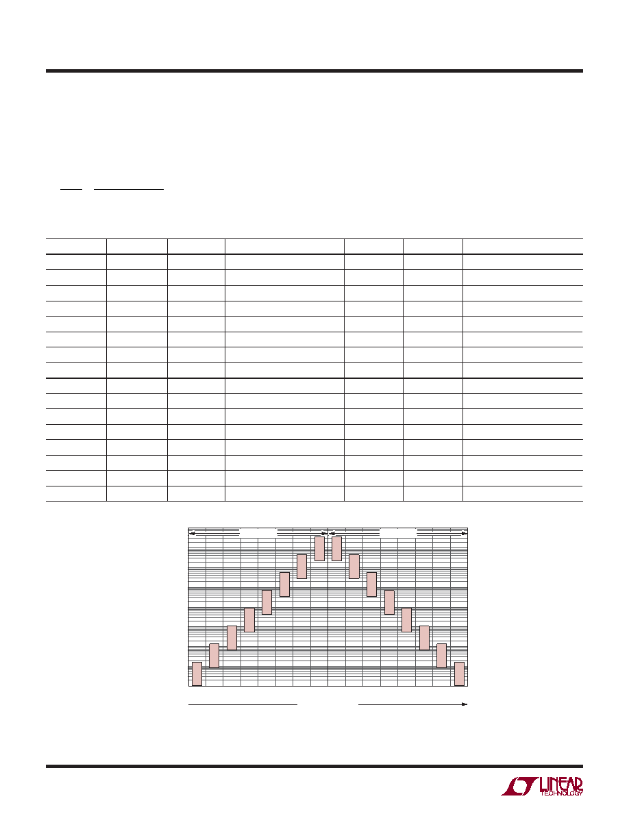
Figure 2. Delay Range and POL Bit vs DIVCODE
If the voltage is generated by other means (i.e., the output
of a DAC) it must track the V+ supply voltage. The last
column in Table 1 shows the ideal ratio of VDIV to the
supply voltage, which can also be calculated as:
VDIV
V+
=
DIVCODE
+ 0.5
16
±1.5%
Forexample,ifthesupplyis3.3VandthedesiredDIVCODE
is 4, VDIV = 0.281 3.3V = 928mV ± 50mV.
Figure 2 illustrates the information in Table 1, showing
that NDIV is symmetric around the DIVCODE midpoint.
0.5V+
t DELA
Y(ms)
699412 F02
1000
10000
100
10
1
0.001
0.1
0.01
INCREASING VDIV
V+
0V
POL BIT = 0
0
1
2
3
4
5
6
7
8
9
10
11
12
13
14
15
POL BIT = 1
发布紧急采购,3分钟左右您将得到回复。
相关PDF资料
LTC7541ABN#PBF
IC CMOS D/A CONV 12BIT 18-DIP
LTC7545ACG#TRPBF
IC D/ACONV MULTIPLY 12BIT 20SSOP
LTC8043EN8
IC D/A CONV 12BIT SERIAL 8-DIP
LTC8143ESW#TRPBF
IC D/A CONV 12BIT SERIAL 16-SOIC
LTM9011CY-14#PBF
IC ADC 14BIT UMODULE 140BGA
LV5609LP-E
IC CLOCK DRIVER VERTICAL 24VCT
LV5609LP-TE-L-E
IC CLOCK DRIVER VERT VCT24
M-986-2A1PL
IC TRANSCEIVER MF 2CHAN 44-PLCC
相关代理商/技术参数
LTC6994CDCB-2TRMPBF
制造商:LINER 制造商全称:Linear Technology 功能描述:TimerBlox: Delay Block/ Debouncer
LTC6994CS6-1#PBF
制造商:Linear Technology 功能描述:SC-Timing, Cut Tape Delay with Rising or Falling Edge Trigger
LTC6994CS6-1#TRMPBF
功能描述:IC DELAY LINE TSOT-23-6 RoHS:是 类别:集成电路 (IC) >> 时钟/计时 - 延迟线 系列:TimerBlox® 标准包装:2,500 系列:- 标片/步级数:- 功能:多个,不可编程 延迟到第一抽头:10ns 接头增量:- 可用的总延迟:10ns 独立延迟数:4 电源电压:4.75 V ~ 5.25 V 工作温度:0°C ~ 70°C 安装类型:表面贴装 封装/外壳:14-SOIC(0.154",3.90mm 宽) 供应商设备封装:14-SOIC 包装:带卷 (TR)
LTC6994CS6-1#TRPBF
功能描述:IC DELAY LINE TSOT-23-6 RoHS:是 类别:集成电路 (IC) >> 时钟/计时 - 延迟线 系列:TimerBlox® 标准包装:2,500 系列:- 标片/步级数:- 功能:多个,不可编程 延迟到第一抽头:10ns 接头增量:- 可用的总延迟:10ns 独立延迟数:4 电源电压:4.75 V ~ 5.25 V 工作温度:0°C ~ 70°C 安装类型:表面贴装 封装/外壳:14-SOIC(0.154",3.90mm 宽) 供应商设备封装:14-SOIC 包装:带卷 (TR)
LTC6994CS6-1TRMPBF
制造商:Linear Technology 功能描述:Delay Block/Debouncer 1us-33.6s TSOT23-6
LTC6994CS6-2#PBF
制造商:Linear Technology 功能描述:DELAY BLOCK/DEBOUNCER 5.5V T 制造商:Linear Technology 功能描述:DELAY BLOCK/DEBOUNCER, 5.5V, TSOT-23-6; Operating Mode:Monostable; Supply Voltage Min:2.25V; Supply Voltage Max:5.5V; Digital IC Case Style:TSOT-23; No. of Pins:6; Clock External Input:Yes; Operating Temperature Min:0C ;RoHS Compliant: Yes
LTC6994CS6-2#TRMPBF
功能描述:IC DELAY LINE TSOT-23-6 RoHS:是 类别:集成电路 (IC) >> 时钟/计时 - 延迟线 系列:TimerBlox® 标准包装:2,500 系列:- 标片/步级数:- 功能:多个,不可编程 延迟到第一抽头:10ns 接头增量:- 可用的总延迟:10ns 独立延迟数:4 电源电压:4.75 V ~ 5.25 V 工作温度:0°C ~ 70°C 安装类型:表面贴装 封装/外壳:14-SOIC(0.154",3.90mm 宽) 供应商设备封装:14-SOIC 包装:带卷 (TR)
LTC6994CS6-2#TRPBF
功能描述:IC DELAY LINE TSOT-23-6 RoHS:是 类别:集成电路 (IC) >> 时钟/计时 - 延迟线 系列:TimerBlox® 标准包装:2,500 系列:- 标片/步级数:- 功能:多个,不可编程 延迟到第一抽头:10ns 接头增量:- 可用的总延迟:10ns 独立延迟数:4 电源电压:4.75 V ~ 5.25 V 工作温度:0°C ~ 70°C 安装类型:表面贴装 封装/外壳:14-SOIC(0.154",3.90mm 宽) 供应商设备封装:14-SOIC 包装:带卷 (TR)